|
DIGITAL LOGIC TRAINER
Delivers all of the functions you need to explore the theory and operation of digital and microprocessor IC's
NEIL J. BUNGARD
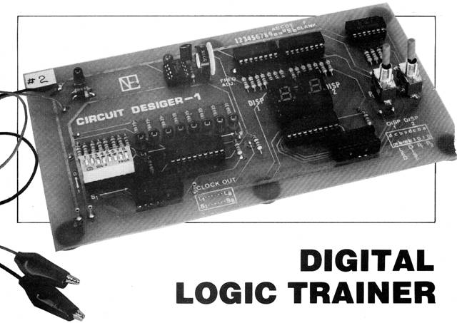
THERE HAS BEEN AN INCREASING NUMBER OF DIGITAL cookbooks and books related to the training of digital and microprocessor techniques appearing on the market. With this increase in literature it becomes desirable to find an affordable device to supply and monitor the functions necessary to explore the theories and operations of digital and microprocessor IC's The Circuit Designer-I is such a device. It can be used as an aid in training digital and microprocessor techniques but will also double as a prototyping aid in circuit design and IC investigation and testing.
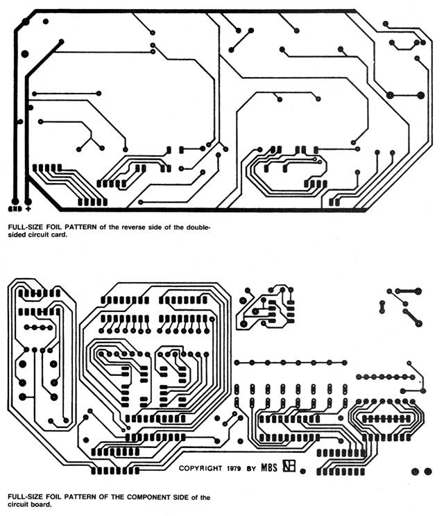
Circuit Designer-I is configured in two separate PC boards: a digital techniques board and a microprocessor techniques board. They can be used independently or combined to complement one another. Since the two boards can be used as stand-alone units I will explain their functions and their use independently.
Circuit description
In this article I will focus on the digital techniques board that consists of 8 logic-level switches. 8 (input latchable) logic-level indicators, a variable-frequency square-wave generator, 2 (input-latchable) decoded seven-segment displays, and 2 debounced-pulsers with complementary outputs.
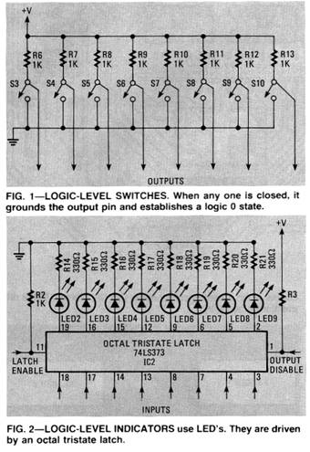
The logic-level indicators (Fig. 2) consist of an octal tristate latch which has its outputs tied to light-emitting diodes through current-limiting resistors to ground. In the normal condition (that is with no input control signals connected) the output disable pin is tied to through R3, holding the output enabled. The latchenabled pin is tied to ground through R2, maintaining the latch disabled, which means that the 74LS373 is transparent and the outputs will follow the inputs.
The variable frequency clock is a basic 555 oscillator circuit (Fig. 3). The oscillator, is variable via R1 but since the frequency is dependent upon Rt and Ct (FREQ = 1. .44 / RtCt)) the dynamic range can be varied by your choice of Ct With the values provided on my board the limits you can expect are between 0.5 Hz and 20 Hz.
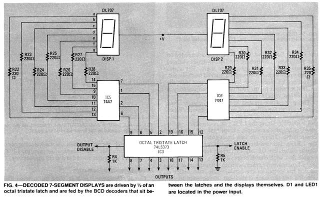
The decoded seven-segment displays (Fig. 4) consist of an octal tristate latch (each display using half of the 74LS373) whose outputs are tied to a set of BCD)-to seven-segment decoders (7447’s). The decoders are tied through current-limiting resistors to common-anode seven-segment displays. The normal condition of the seven-segment octal latch is exactly the same as the logic-indicator octal latch. The inputs are enabled and the latches disabled, which means that the 74LS373 appears transparent.
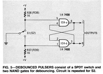
The debounced pulsers (Fig. 5) consist of a SPDT momentary switch and the NAND gates for debouncing. the circuit utilizes the fact that a TTL gate has a definite signal propagation time (about 10 ns for a NAND gate) to filter out the contact bounces. Using Circuit Designer-I
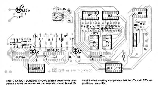
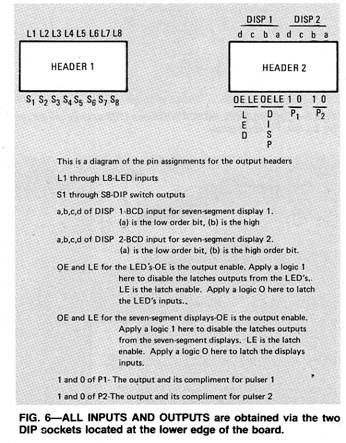
On the digital techniques board all the inputs and outputs are obtained via two DIP header sockets (see Fig. 6) on the lower edge of the board (with the exception of the power and oscillator outputs, which are taken from individual wire-insert sockets).
Operation of the state-switches, oscillator, and pulsers are straightforward. Just run the outputs from the Circuit Designer-I to wherever they are needed on the breadboard. Switching the DIP switches changes the states at the pins assigned to them. The states related to the switch positions are marked on the board. If you need a clock pulse just run a jumper from the oscillator output pin to your circuit. The frequency is variable via variable resistor on the board.
The pulsers are treated in the same manner. Run jumpers from the pulser outputs to your circuit. When you depress the pulser the pins will change states without bouncing. Using the LED’s or seven-segment displays is equally as simple except that the inputs are controllable. There are two input-control signals for the LED’s and two identical signals for the displays. These signals are OE and LE, which represent output enable and latch enable respectively.
As I mentioned earlier, with no control signals connected the output of the octal tristate latch buffer is enabled and the latch is disabled. If you want to disconnect the LED’s or seven-segment displays from the octal latch’s output place a logic 1 on OE. If you want to latch the information on the inputs apply a logic 0 on LE. This is very useful when using the LED’s or displays as output ports from a microprocessor.
Miscellaneous information Circuit Designer-I is best used by running DIP header cables from the board sockets to the breadboard and running shorter wires from the header on the breadboard to the circuits under examination. The power supplies that I have been using in my classes are 6-volt lantern batteries which deliver months of reliable service. Also the books that I have found that best complement Circuit Designer-I as a trainer are the “Bugbook” series by Rony, Larsen, and Titus.
In a future article I will introduce Circuit Designer l's microprocessor techniques board. This board is also powered by a lantern battery and connects directly to the digital techniques board. With this device we will be able to investigate microprocessor address and data bus concepts, memory allocation, I/O control, interrupts, machine language programming, and other microprocessor-related concepts.
|
 The
total circuit is basically 5 separate circuits on a single
printed-circuit board. Also provided on the power input is a diode
to protect against applying re verse voltage to the board, and a LED
to indicate a “power on” condition. The logic-level switches (Fig.
1) consist of a pull up resistor to a logic- 1 state. When the
switch is closed it grounds the output pin and establishes a logic-O
state. There are 8 such switches on a single DIP.
The
total circuit is basically 5 separate circuits on a single
printed-circuit board. Also provided on the power input is a diode
to protect against applying re verse voltage to the board, and a LED
to indicate a “power on” condition. The logic-level switches (Fig.
1) consist of a pull up resistor to a logic- 1 state. When the
switch is closed it grounds the output pin and establishes a logic-O
state. There are 8 such switches on a single DIP.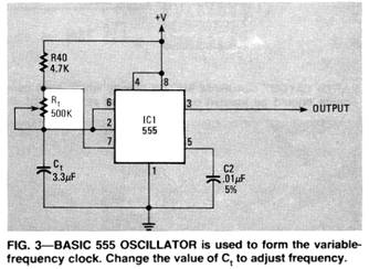
Copyright by Bill Bytheway, K7TTY February 2012